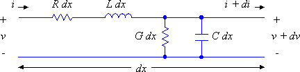
Figure 1: The elemental model for a lossy transmission line.
LABORATORY #6
TRANSMISSION LINE EFFECTS IN HIGH-SPEED LOGIC SYSTEMS
Copyright 2000, Alan V. Sahakian
GOALS:
To learn about the interaction of logic circuits with transmission line interconnections. To continue to learn about the use of high-speed oscilloscopes and probing systems.
OBJECTIVES:
To be able to predict voltages in systems involving transmission lines and logic gates with linear source and load models using the reflection coefficient method.
To be able to predict voltages in systems involving transmission lines
and logic gates with non-linear source and load models using the Bergeron
Diagram method.
COMPONENTS AND INSTRUMENTS REQUIRED:
1 7404 Hex TTL inverter
2 2N3643 (or equivalent) NPN Si transistor
2 100 Ohm 1/4 W resistor (composition
or film)
1 3.3k Ohm 1/4 W resistor (composition
or film)
1 1k Ohm 1/4 W resistor (composition
or film)
1 50 Ohm 1/4 W resistor (composition
or film)
1 Length of RG-58 transmission line
1 IPC Trainer
1 High-speed (60 or 100 MHz) scope with
two 10:1 passive probes
INTRODUCTION:
In this lab you will use two methods to predict voltages and currents at the points of interconnection between logic gates and transmission lines. The first method uses a linear model to calculate a reflection coefficient and is only valid when a linear model applies for both source and load. The second method, called the Bergeron Diagram method, is a graphical technique which is more general and can be used for arbitrary non-linear sources and loads.
First, you will build a simple circuit to measure a transmission line's characteristic resistance and propagation velocity. You will use this to characterize a length of RG-58 coaxial cable. (Although many logic interconnections are microstrip or stripline printed-circuit connections, we have chosen to use a simple coaxial cable which is relatively long to simplify your measurements.) After characterizing your line you will build two circuits, one which is well approximated by linear source and load models, and one which is non-linear. You will predict and then measure the voltage waveforms in these two circuits.
BACKGROUND:
The most general elemental model of a transmission line is given in Figure 1. This element is considered to represent an infinitesimally short section of a transmission line (having length dx).
Figure 1: The elemental model for a lossy transmission line.
Note that this model includes two reactive elements, L and C, and two resistive elements R and G. The resistive elements dissipate energy as heat and make the line lossy. If these elements are removed (i.e. resistance R and conductance G both become infinitely small) then the line is lossless. All of these elements are normalized to a unit length (i.e. L is Henrys per meter, C is Farads per meter, R is Ohms per meter and G is Siemens per meter). The elemental model is considered to have a voltage and current input, v and i, and is adds an increment of voltage and current, dv and di, to its output.
For the lossy case the currents and voltages are described by the following pair of differential equations:
|
|
(i)
|
|
|
|
(ii)
|
For the lossless case the terms involving R and G drop out and the equations become
|
|
(iii)
|
|
|
|
(iv)
|
Equations (iii) and (iv) can be combined to yield the second-order equation
|
|
(v)
|
the solution to which has the form
|
|
(vi)
|
Two constants may be recognized from equations (v) and (vi). The propagation velocity, u, may be calculated as
|
|
(vii)
|
and the characteristic resistance R0 may be calculated as
|
|
(viii)
|
(In the case of a lossy line the line's characteristic impedance Z0 is complex.)
In all of what follows we will be assuming that the transmission lines which we are dealing with are lossless. This assumption is justified if we are dealing with relatively short lines with brief transient responses, which is often the case in well-designed logic systems.
ECE 353 students in EE will take other courses (i.e. ECE 301 and ECE 308) which spend considerably more time on the theory of transmission lines. Here we simply present the solution methods without much justification.
MEASURING u AND R0:
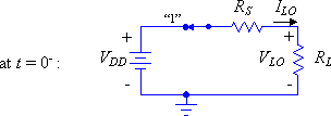
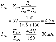
An infinitely long transmission line may be modeled as a single element which represents the characteristic resistance R0 of the line. A finite-length line will behave this way also, but only for the brief time which it takes for energy to travel down and back the length of the line. This fact allows us to measure R0 by a simple method. Using a voltage divider with the transmission line as one component and a known resistance as the other we can calculate R0 by driving the voltage divider with a known-amplitude voltage step and examining the voltage across the transmission line input immediately after the step is applied. From this we can calculate R0 from the voltage divider equation. We'll assume that the voltage and current on the transmission line were both zero for all time preceding the step. The setup for this measurement is shown in Figure 2.
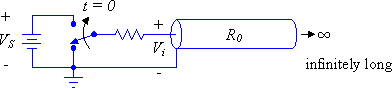
Figure 2: Measuring R0 using a voltage step.
LAB ASSIGNMENT:
Measure R0 for your line using this technique. For your step generator, use six 7404 inverters in parallel (to maximize logic-1 output drive and therefore VS). Measure VS and Vi and calculate RS from these and the known value of RS. The setup is shown in Figure 3 below:
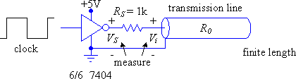
Figure 3: Experimental setup for measuring R0 and u.
Propagation velocity u can be calculated by measuring the physical length of the transmission line (l) and dividing by its measured electrical length (T). The measurement setup for R0 will also yield T. Once R0 and u are known you can calculate values for L and C.
Report values of R0, l, T, u, L and C for your transmission line.
TRANSMISSION LINE REFLECTIONS:
If a transmission line is terminated in its characteristic resistance R0, then the energy in a wave traveling on the line is completely transferred to the load, and no reflection occurs. In the case of different values of R0 and the load resistance RL a reflection will occur and the energy in this will return along the path which the incident wave traveled.
In the case of linear terminations the magnitude of the reflection is proportional to the reflection coefficient, p, which is given by
|
|
|
(ix)
|
If the source's own resistance RS is not equal to R0 then there is a second reflection, and so on.
Intuitively it should be clear that for any practical circuit the traveling energy is eventually dissipated in the source and load resistances. If these are nearly zero or infinite, however, the reflection coefficient will be nearly -1 or 1 respectively, and if the line is nearly lossless the traveling wave can bounce from end to end for a long time.
In general the goal in designing digital systems involving transmission lines is to ensure that the initial traveling wave is largely dissipated in either the load or source end. In this way the line voltage will reach its final value when the first traveling wave arrives (at T).
REFLECTION CALCULATIONS:
Whenever a traveling wave voltage step on the line encounters the source or load the following model must be used to solve for the resulting voltage and current:
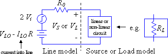
Figure 4: Transmission line model used at t = T, 3T,
5T, etc. at load end
and at t = 0, 2T, 4T, etc. at source end.
The model must also be used at t = 0 to calculate the initial step launched on the line. The quantities VLO and ILO are the initial voltage and current on the line (i.e. just before the step arrives, or at t = 0- in the case of the initial step). If the system involves only resistances (linear source and load model) then we can calculate the reflection coefficients for source and load ends (pS and pL) and from this calculate the reflected voltages without solving the circuit in Figure 4 at every time step. If the source and or load are not linear then no single value of p can describe it and we must resort to a method like the Bergeron diagram which is essentially a graphical solution for the model in Figure 4 applied alternately to source and load.
METHOD FOR LINEAR-MODEL SOURCE AND LOAD CIRCUITS:
This method involves the following steps:
1) Calculate the initial voltage step (at time t = 0) using the model shown in Figure 4, including any initial conditions.
2) Calculate the reflected voltages at load end at times T, 3T, 5T, etc. and at source end at times 2T, 4T, 6T, etc. using the equation
|
|
(x)
|
3) For each time calculate the voltage at the corresponding end as the voltage at that end plus the voltage arriving plus the voltage reflected using the equation
|
|
(xi)
|
Because of all of the calculations it is helpful to have a method of organizing the process. The "reflection diagram" is such a method. In a reflection diagram horizontal position represents distance along the line and vertical position represents time, with increasing time moving downward on the diagram. Diagonal lines are drawn representing traveling waved (voltage steps) moving from end to end. In general, when a diagonal line meets a time axis at source or load end, a traveling wave is arriving and another will be reflected; this will happen at T, 2T, 3T, etc.
An example reflection diagram is drawn for you in Figure 5.
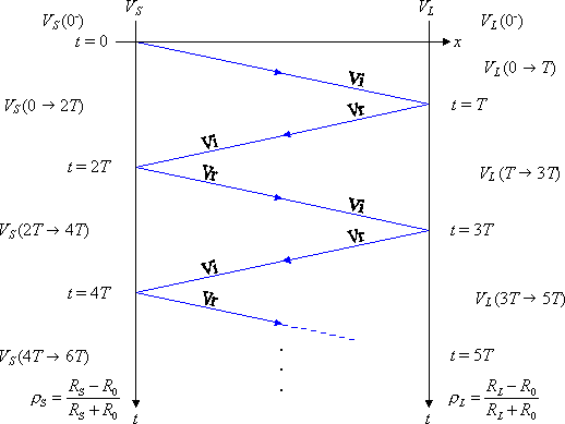
Figure 5: A transmission line circuit and the corresponding reflection diagram.
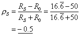
A typical problem involving a transmission line and linear source and load model is worked for you below:
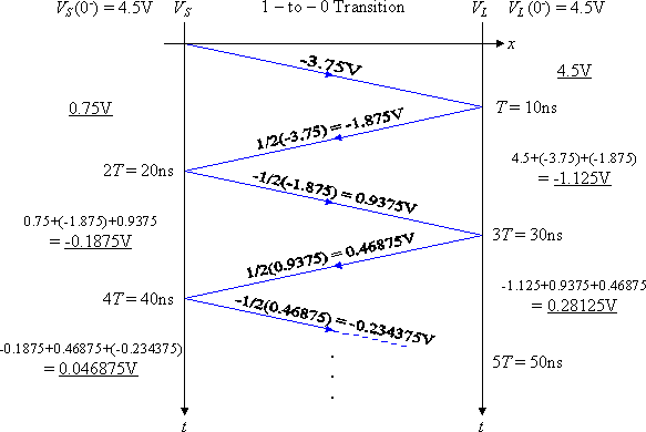
Given the following circuit, calculate the voltages at the source and load ends of the transmission line from t = 0- to 40ns (4T).

 |
 |

 |
|
 |
![]()
Figure 6: An example of a solution using the reflection diagram method.
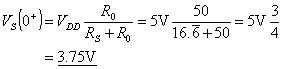
The voltage waveforms are plotted in Figure 7.

Figure 7: Source and Load voltages VS and VL for the worked example.
 |
 |
 |
![]()
Figure 8: Example solution for the 1-to-0 transition, which has non-zero
initial conditions.
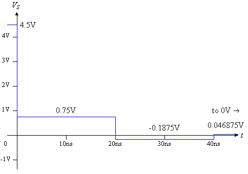

Figure 9: VS and VL for the 1-to-0 transition for the worked example (from Figure 8).
LAB ASSIGNMENT (reflection coefficient method):
(Note: for these measurements you must use a bypass capacitor across the IC and use proper probing techniques, including compensating the probe and using short and direct connections for both the probe tip and the ground lead. Without these measures you will find it difficult to see the waveforms due to ringing and other parasitic effects.)
1) Using the reflection coefficient method, solve the cases for the 0-to-1 and 1-to-0 transitions when RS is 1k Ohm and RL is infinite (and R0 is the characteristic resistance which you measured for your line). Verify your solution by building the circuit (actually it's already built) and measuring voltages. Is your calculated response correct? What are possible sources of error?
2) Repeat (1) for RL = 0 Ohm.
3) Repeat (1) for RL = R0
NON-LINEAR SOURCE/LOAD MODELS AND THE BERGERON DIAGRAM:
Often in digital systems the source and load models are not linear; that is the relationship between current and voltage at the output of the source, and/or the input of the load, is not linear. In this case there is no single reflection coefficient which describes the source or load. An elegant graphical method, called the Bergeron Diagram method, has been developed and is widely used to handle these cases. This method applies the model of Figure 4 alternately at source and load ends to find the solutions as the traveling wave bounces from end to end. Very conveniently, the solution method keeps track of the initial line current and voltages VLO and ILO automatically, as well as the amplitude of the traveling wave, and allows us to read out both the voltage and current at source and load at any moment in time. The Bergeron Diagram method works for the case of linear source and load as well. This method will be presented here without much theoretical justification but, as mentioned before, in ECE 308 the background is covered in detail.
The solution is based on a graphical construction. The voltage-current relationships for both source and load are plotted together on a single graph. For convenience that graph should be scaled such that a slope of 45° corresponds to a conductance of 1/R0. In other words if the voltage axis is scaled such that 1cm on the graph corresponds to 1V, then the current axis should be scaled such that 1cm corresponds to the current which would flow through a resistance of R0 with 1V across it (i.e. 1V/R0).
In general there will be two source models, and therefore two source V-I curves to deal with, one for the logic-0 case and another for the logic-1 case. Note that the intersection of a source and load curve corresponds to the steady-state (DC) solution for the circuit.
After all the reflections have died out, the circuit should be operating at such an intersection. During the transient solution the transmission line model of Figure 4 is graphically applied alternately at source and load end to find the currents and voltages which apply at a given moment in time at source and load. This transmission line model is simply a + or - 45° line which passes through the operating point from the previous time step. Following this method alternately at source and load we should eventually converge on the steady-state operating point of the circuit. This process is much easier to show in an example than it is to describe in text. Figure 10 presents the solution to the example of Figure 6 using the Bergeron Diagram method. The source and load models are straight lines in this example, since they are both linear circuits, but the method applies to both linear and non-linear circuits.
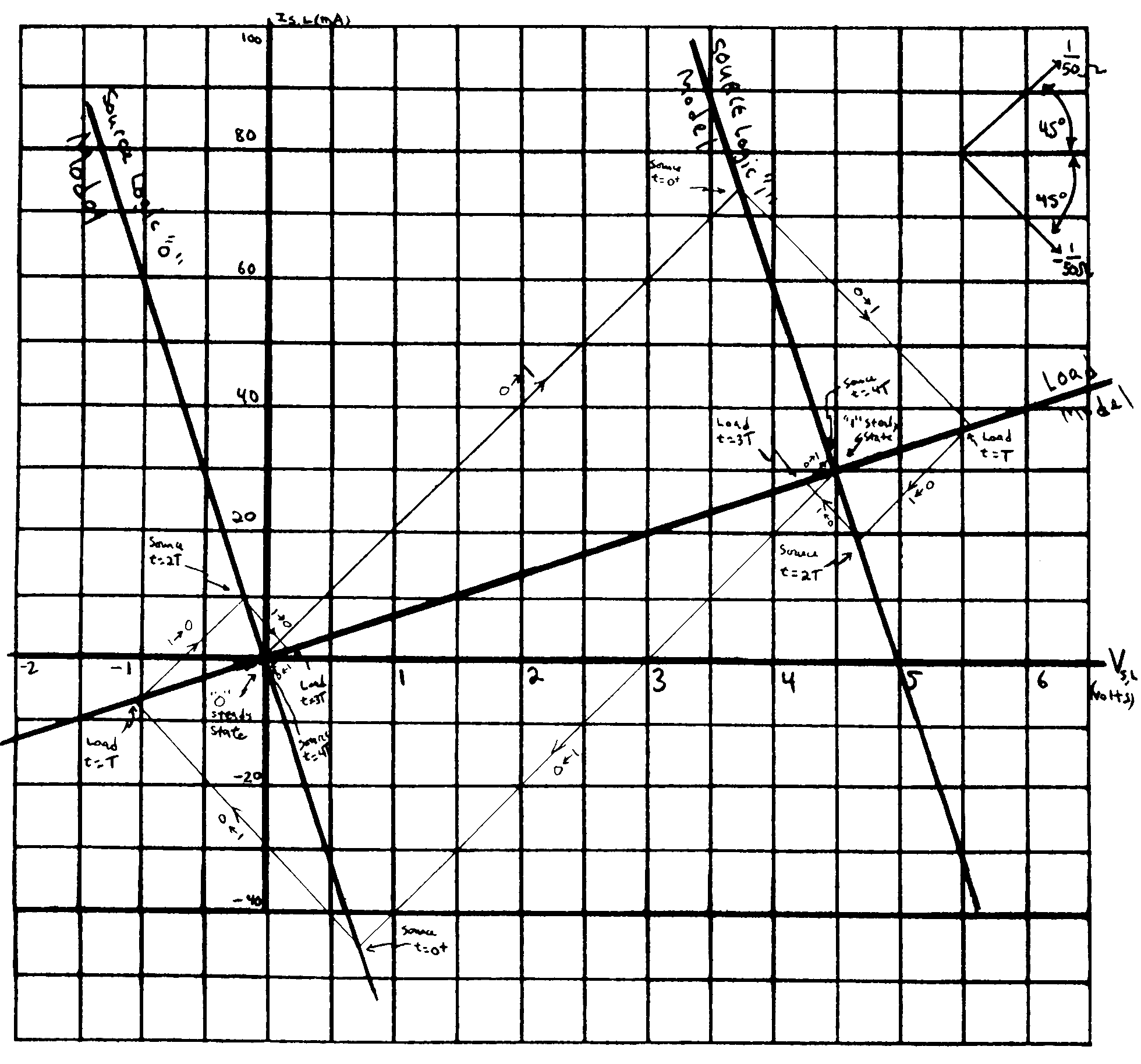
Figure 10: The example of Figure 6 worked using the Bergeron Diagram method.

LAB ASSIGNMENT (Bergeron Diagram method):
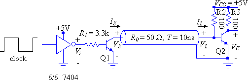
Construct the circuit below. Using the Bergeron diagram method predict the voltages at source and load end, VS(t) and VL(t), and the output of the final inverter at the collector of Q2, VC2(t). The characteristics of Q1 and Q2 are presented graphically on the next page (curve-tracer displays), and you can re-draw these using straight-line approximations to make constructing your Bergeron Diagram easier. You can assume that the transmission line's characteristic resistance is 50 Ohm. Measure these voltages in your circuit and compare with the predicted voltages. What are the possible sources of error?
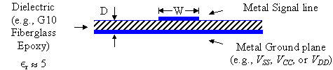
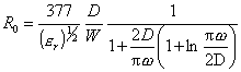
Characteristic Impedance of Printed-Circuit Board traces over Ground (microstrip).

Collector-Emitter Characteristics, Stepped Base Current
2N3643 Ic: 2mA/div, VCC:
2V/div
Ib = 0, 20µA, 40µA, ...
Base-Emitter Characteristics
2N3643 Ib: 2mA/div, Vbc:
0.5V/div